Over the years, academics developed a variety of systems that you could run quantum algorithms on. Most of these had one or two helpful traits—easy to manipulate or able to hold their state for longer—but lacked enough of the others to keep them from being practical computing solutions. Over the last few years, however, a number of companies have figured out how to manufacture significant numbers of solid-state qubits called transmons. Because the fabrication technology for transmons is similar to that of existing chipmaking, lots of the major players in the nascent market—including Google, IBM, and Rigetti—have settled on transmons.
But transmons aren’t ideal either. They require extremely cold temperatures, show significant device-to-device variability, and are good but not great at holding their state. A number of people in the field I’ve talked to have suggested there’s still room for another technology to surpass transmons, and Ars’ own Chris Lee is putting his money on that happening.
Now, a company new to the quantum computing market is also betting it will. Honeywell, a company better known as a defense contractor and materials supplier, is announcing that it has built a quantum computer using an alternate technology called “ion trap” and will be making it available via Microsoft’s Azure cloud service later this year. The company also claims that, by some measures, it’s the most powerful quantum computer yet built, but that’s a claim that needs to be considered very carefully.
Transmon qubits work by circulating a current through a loop of superconducting wire, linked to a resonator that allows the state of the current to be controlled and read out. Both the superconducting wire and resonator, however, have to be manufactured, which allows for subtle differences between the individual qubits. In addition, all of that hardware has to be kept extremely cold—within a tiny fraction of a percent of absolute zero—in order to keep these relatively large objects near their quantum ground state.
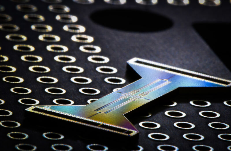
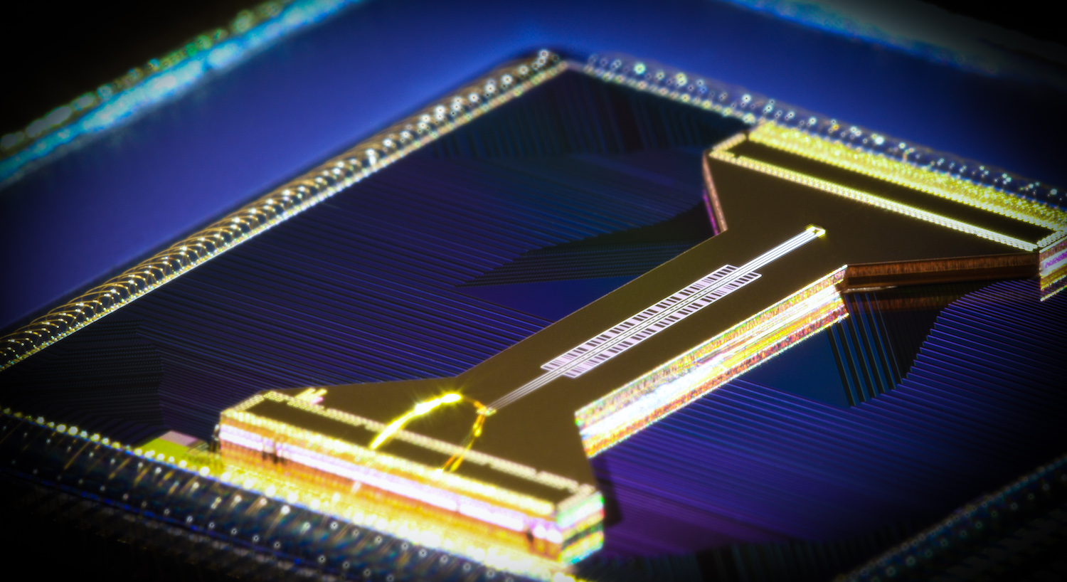
Trapped ions provide a way around some of these challenges. The actual qubit is formed from a very small number of atoms—just two in Honeywell’s case. Honeywell’s president of Quantum Solutions, Tony Uttley, emphasized to Ars that this eliminates manufacturing issues, as every single device has identical properties defined by the atom being used (ytterbium in this case). “Every qubit starts perfect,” Uttley told Ars. “Any error that you introduce is an error that you’ve put in place because of the surrounding infrastructure.”
Because of Honeywell’s experience with making and integrating this infrastructure, the company’s engineers feel that they were in a great position to minimize this noise. The other thing is that small clusters of atoms like these can be cooled using lasers. While the environment has to be kept very cold, it doesn’t have to reach the extreme temperatures needed by a transmon.
In Honeywell’s case, the ytterbium ions weren’t especially easy to cool using lasers, so they threw a couple of barium ions in the mix and cooled those with lasers. The ensemble of four ions was easy to cool and control, and the environment only had to be kept at 12K. This does require liquid helium but not the elaborate dilution refrigeration systems needed for Google and IBM’s hardware.
Because they’re charged, the ions can be moved within the device simply by changing the local electric fields using the roughly 200 electrodes arranged along the device. The state of the ion’s electrons can be manipulated with lasers at specific wavelengths, which can put electrons in a superposition of potential energy states. Entanglement and various gate operations can be achieved simply by moving two ions into close proximity and by using laser operations that manipulate both simultaneously. Readout is achieved by stimulating the ions with yet another laser, which will cause the ions to emit a photon that’s indicative of their state.
Honeywell’s hardware can be seen as a linear string of distinct devices. Ions enter at one end and are shuffled along through alternating regions where they can be held for storage or hit by lasers that perform qubit manipulation operations on them. A gate operation (the quantum equivalent of performing an AND or NOT operation) can be done by simply placing two ions in the same location and performing an operation on both of them simultaneously. In addition, clusters of four ions (two ytterbium, two barium) can be split in half, or two clusters of two ions can be merged.
The device Honeywell is describing today lines up four qubits along a single line of these storage/manipulation stages. But the diagram of the device also shows two additional lines of storage and manipulation stages flanking the line that was used in these initial experiments. This is in keeping with what Uttley told Ars: Honeywell is convinced the device can scale rapidly, with the expectation that additional qubits can be added each year without a fundamental change in architecture. So, while four qubits is quite low compared to what has been achieved with transmon devices (more on that in a bit), the company is expecting that it can narrow the gap very quickly.
One interesting aspect of this setup, which Uttley says isn’t available on any other commercial system right now, is that you can measure a qubit individually without necessarily disturbing anything else in the system. (Technically, this is done by a science fiction-sounding operation called a quantum-teleportation CNOT gate.) This allows the computer to perform the equivalent of an “if” statement, changing the algorithm based on the results of measuring this single qubit. After measurement, the qubit can also be reset and reused for further computation.
Individual components of this perform extremely well. One potential issue is what are called “state preparation and measurement errors,” which have picked up the acronym SPAM. In this case, Honeywell’s researchers find that the SPAM is dominated by measurement errors, but those occur less than 1 percent of the time. Single qubit gates have errors about an order of magnitude lower, and two-qubit gates are on a similar level. All of these are considerably lower than the typical behaviors of transmon gates.
Honeywell is announcing this as “the world’s most powerful quantum computer,” but that claim depends very strongly on the benchmark used. In this case, Honeywell is using a measure defined by IBM, which termed it “quantum volume.” We’re going to quote part of Chris Lee’s analysis of quantum volume here, because it very much captures how this relates to Honeywell’s computer.
Because quantum gates can always introduce an error, there is a maximum number of operations that can be performed before it is unreasonable to expect the qubit state to be correct. Circuit depth is that number, multiplied by the number of qubits. If used honestly, this provides a reasonable idea of what a quantum computer can do.
The problem with depth is that you can keep the total number of qubits constant (and small), while reducing the error rate to very close to zero. That gives you a huge depth, but only computations that fit within the number of qubits can be calculated. A two-qubit quantum computer with enormous depth is still useless.
The goal, then, is to express computational capability, which must include the number of qubits and the circuit depth. Given an algorithm and problem size, there is a minimum number of qubits required to perform the computation. And, depending on how the qubits are connected to each other, a certain number of operations have to be performed to carry out the algorithm. The researchers express this by comparing the maximum number of qubits involved in a computation to the circuit depth and take the square of the smaller number. So, the maximum possible quantum volume is just the number of qubits squared.
As noted above, Honeywell’s reported error rates are very low, which means that each calculation run on its four qubits is likely to be error-free. And, because the ions can be moved around the device at will, any of them can be arbitrarily connected to any others. Thus, the quantum volume is actually equal to the number of qubits squared here. That’s in contrast to the hardware being used by the likes of Google and IBM, which have over 10 times the number of qubits but also have appreciable error rates and qubits that are only connected to a handful of their nearest neighbors.
As a result, it wouldn’t take adding many more qubits for Honeywell’s machine to have a larger quantum volume than those of its competitors. And, as noted above, the hardware it’s describing today definitely has the built-in capacity for added qubits. So, it’s claiming a quantum volume of 64, which would mean eight qubits, and there’s reason to believe the company can deliver.
But with IBM already offering a computer with nearly 64 actual qubits, and Google poised to follow, does eight qubits really matter? The answer, as always on these things, is “it depends.” Some algorithms are going to be very sensitive to the connectivity among the qubits. While it’s possible to run them on larger machines with lower connectivity, doing so requires more qubits acting as bridges to establish the equivalent connectivity, and each of those comes with the potential for introducing an error. For Honeywell’s machine, the higher connectivity could offset some of the need for additional operations, and the operations aren’t the major source of error anyway.
There’s also the issue of scaling. Uttley told Ars that he expects that the company can increase its quantum volume by an order of magnitude a year for the next five years, which means adding three or four qubits a year. That means that, even at the five-year mark, it would only be at about 30 qubits—about half of where its competitors are today. Meanwhile, Google and IBM are working on bringing error rates down and have been adding a couple dozen qubits to their machines every few years.
If all the companies see their plans work out, things will get very interesting within a few years. Honeywell will having a substantial lead in quantum volume, while its competitors’ transmon-based hardware has an order of magnitude more qubits. Meanwhile, team transmon is aiming for error-corrected quantum computing, which will require thousands of qubits—which means the researchers expect that, at some point, they’ll be able to add hundreds of qubits with each new generation of chips.
Since it’s not clear when these other companies expect this qubit growth count to take off, there’s no way to guess how Honeywell’s entry might change the competitive landscape here.
Honeywell, a company that boasts divisions devoted to everything from sporting goods to defense contracting, is definitely an unusual entry in a market that has been dominated by a mix of startups and traditional computing powerhouses. But the company has told a consistent origin story, one that was reiterated by Uttley: as part of its materials and manufacturing work, Honeywell had developed many of the pieces needed for ion trap computing, like photonics, cryogenics, and vacuum systems, for other purposes. And a group of scientists within the company argued that the potential of the field was large enough to be worth pursuing. And, because Honeywell is such a large company to begin with, it was able to create a substantial group devoted to developing the project.
Like everybody else in this business, Honeywell has determined that most companies aren’t interested in setting up the infrastructure needed to run their own liquid-helium cooling system. So, Honeywell is going to be offering access to its quantum computers via a cloud interface. It has also partnered with Microsoft to make the system accessible via that company’s Azure cloud service.
For writing the actual software used in the work done today, Honeywell’s researchers adopted IBM’s Quiskit, an open source tool that allows quantum algorithms to be described in a hardware-agnostic manner and then generates the actual commands needed for the hardware actually being used (it’s a bit like a cross-platform compiler). So, the company is hoping to leverage some of the existing expertise that has already developed there. It also could mean that companies can develop a set of quantum algorithms, then choose to run them on whatever system has the features they need—high connectivity or high qubit count—to achieve the performance needed.
Presumably because it’s introducing a completely new architecture, the company paired today’s hardware announcement with two investments in companies that are already involved in quantum algorithm development. It’s also announcing that the financial giant JPMorgan Chase will be working with Honeywell to explore the use of its system for financial algorithm development. This should not be taken as an indication the system is ready for use; we’ve talked to people at JPMorgan Chase in the past, and they’ve indicated their efforts are being made to ensure the company is fully prepared when quantum computing is ready for prime time.
All of this indicates that Honeywell is definitely taking this effort seriously and hopes to be a major competitor in the quantum computing space. And, if its projections of future performance gains turn out to be accurate, it very much could be.
An observer might be tempted to view this as something akin to the competition among traditional computing architectures, where x86 and ARM are currently heavily competitive. But those different architectures are produced using the same processes and operate using individual components that are identical. Here, the two competing architectures are based on completely distinct physical systems that just happen to obey some of the same rules. That’s a very different set of circumstances, and one that seems more exciting.
 +1-786-628-7980
 Sign Up/Sign In